


Infrared cameras in electronics development
Temperature measurement of the smallest components
There has been a distinct trend in electronics development in the last few years: packing density is increasing. Today, modern smartphones are much more powerful than they were only a few years ago, yet they are no bigger. The same applies to IT devices, automobile electronics and consumer electronics. Accordingly, problems caused by heating must be looked out for with great care. Modern infrared measurement technology is an important aid in this regard.
As early as 1965, Gordon Moore postulated the rule of thumb which today is generally known as Moore’s law, i.e. that the integration density of semiconductor devices would double every 18 months. The ever-increasing power of semiconductors resulting from this was the basis for the development of modern IT and digitalization which dominate practically every area of our daily lives today
Power loss generates heat
The ever-increasing integration density, however, means that the amount of heat resulting from power loss in the components increases all the time. Another factor here is continual miniaturization, which can impede efficient heat dissipation. Even applications which carry relatively large currents are becoming more and more common – in drive technology for example – thanks to the use of power electronics. The lifespan of semiconductor elements is hugely dependent on temperature. An increase in temperature of 10 °C will cause a 50% reduction in lifespan. This means that developers of electronic assemblies are faced with the challenge of allowing for the thermal behavior of circuit boards and assemblies.
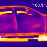
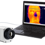
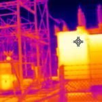
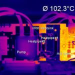
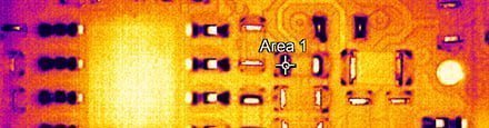
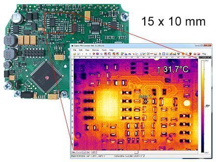
The temperatures of semiconductors, printed circuit boards or entire assemblies are ideally measured with the help of infrared technology. The measuring procedure is quick, precise and non-contact – a consideration of particular importance in electronics manufacturing. When measuring, checks should be made to see where exactly a circuit board is showing which temperatures. The causes for excessive temperatures can be manifold: defective components, incorrectly dimensioned circuit paths or poorly soldered joints. In order to properly record the temperatures of very small components and structures on a circuit board, an infrared camera with a suitably high resolution is necessary. With this you can, for example, identify exactly which component on a circuit board is displaying excessive temperatures.

Infrared cameras are used in various phases of electronics development. Often, temperatures on a printed circuit board are simulated in advance using thermal model calculations. When measuring prototypes these model calculations can then be verified. Should any discrepancies arise, the data gathered during measurement can in turn be included in the simulations to improve the models. When measuring prototypes, components which consume an excessive amount of energy can be identified. This allows errors in the circuit design to be spotted at an early stage. The mutual interference of components on the circuit board can also be detected.
In production, assemblies from external suppliers are often used. To carry out incoming quality control of these assemblies, infrared measurement technology is also used here. This control can be carried out on all items, or by means of random sampling. Infrared cameras are also employed in the final inspection as part of the quality assurance of finished assemblies or circuit boards. This allows faulty components or assemblies, for example, to be identified during burn-in tests.
Choosing the right infrared camera
The ever-increasing integration density, however, means that the amount of heat resulting from power loss in the components increases all the time. Another factor here is continual miniaturization, which can impede efficient heat dissipation. Even applications which carry relatively large currents are becoming more and more common – in drive technology for example – thanks to the use of power electronics. The lifespan of semiconductor elements is hugely dependent on temperature. An increase in temperature of 10 °C will cause a 50% reduction in lifespan. This means that developers of electronic assemblies are faced with the challenge of allowing for the thermal behavior of circuit boards and assemblies.
The more pixels an image sensor has, the higher the possible resolution. However, because the individual bolometers get smaller as the number of pixels increases, the thermal radiation emitted by each pixel is lower. For this reason, smaller pixels need much higher detectivity in order to achieve the same temperature resolution. This places very high demands on thermal isolation, temperature coefficients as well as effective utilization of the sensor surface. In practice, a lower frame rate is used in order to integrate the image signals over a longer time period. In general it is found that the number of pixels, frame rate and temperature resolution cannot be increased independently of each other.
Influence of the lens
As with photo or video cameras, the image sensor (or its pixel count) is not exclusively responsible for high-quality images. The lens plays an equally important role. The lenses of infrared cameras often have a high luminosity. In order to utilize as much thermal radiation as possible while at the same time remaining free of atmospheric influences, all work is carried out in the spectral range of 8 µm to 14 µm. Here, however, you are already entering the pixel size range, so that in the case of very small objects which are only 3 x 3 pixels, for example, the temperature measured is often too low. In order to reliably identify temperatures, the measurement accuracy of the system needs to be provided for small objects as well. Otherwise a high resolution is not much use with regard to the pure number of pixels. As well as ascertaining which is the smallest discernible structure, there is also the important question of the minimum size that an object needs to have in shot in order to reliably determine its temperature.
If the resolution is limited to a low number of small pixels, smaller lenses with a short focal length can be utilized in visual fields of standard size. These are more cost-effective but have the disadvantage that the smaller aperture lets in less light. This, in turn, needs to be compensated by proportionately more sensitive sensors. The visual field of the thermal imaging camera is also dependent on the chosen lens and can range from 6° to 90°. The further the distance between the camera and the object, the larger the captured image region and, as a result, the image detail that an individual pixel can display. The optical resolution of the measuring device must therefore be selected depending on the size of the measurement object and the distance between it and the sensor. To sum up it can be said that a thermal imaging camera’s lens and sensor need to be suitable for the measurement task at hand, while also matching in terms of quality in order to get a thermal image that has both a good thermal and geometric resolution.
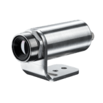
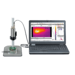
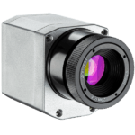
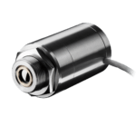
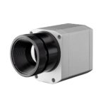
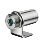
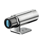
The optris PI 450i und PI 640i infrared cameras are ideally suited to the measurement of electronic assemblies. They feature detector sizes of 382 x 288 pixels (PI 450) and 640 x 480 pixels (PI 640). With the exchangeable and focusable microscope lens [picture 2: microscope lens] you can also capture very small components or structures on a circuit board. The smallest measurement spot diameter is 42 µm in size for the PI 450 and as small as 28 µm for the PI 640. Temperatures are measured with an accuracy of ±2 °C. With the maximum possible frame rate of 125 Hz, fast processes can also be made visible. Both infrared cameras take both pictures and videos which can be analyzed with the license-free analysis software.

Temperature under control
Infrared cameras are a valuable aid in the development, testing and manufacturing of electronic assemblies. With high resolutions, the temperatures and temperature distributions of even miniaturized components can be measured. This helps in spotting errors during the design process and reliably identifying faulty components. The result is quicker and safer electronics development.
